
MTP Applications
INTEGRATION OF COMPOUND SEMICONDUCTORS
Heterogeneous integration of compound semiconductors is a critical technology for advanced wireless communication, power management, optoelectronics and photonics, and sensor components. These have different requirements than logic and memory components.
Micro-Transfer Printing provides:
- Tight integration of large arrays of compound semiconductors (e.g., GaN, GaAs, SiC, SiGe, InP) with silicon (CMOS) semiconductors and passive components (inductors and capacitors) versus integration of chips having standard interfaces and made using different CMOS nodes.
- Lower I/O density and higher current density interconnects.
- Ultra-thin, small footprint three-dimensional integrated circuits (3D ICs) versus a large footprint system-in-package (SiP).
- Disruptive innovations that improve performance but don’t require scaling to advanced CMOS nodes or high I/O density silicon advanced packaging.
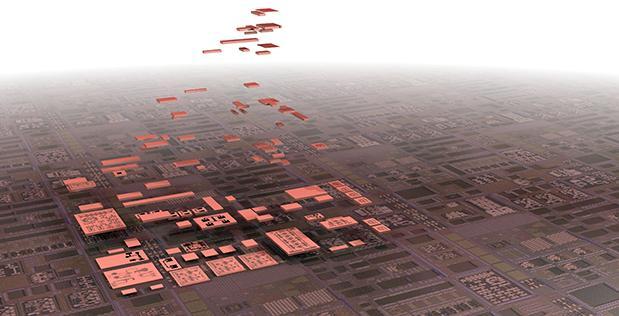

Inserting 3D IC compound semiconductor heterogeneous integration between wafer fabrication and packaging (Figure 1 ) enables many opportunities for disruptive innovation. 3D ICs improve the interconnects (reducing parasitics components, improving thermal management and power density) and bridge the dimensional gap between the wafer fabs’ ultra-fine (<1/1mm line/space) and packaging’s coarse (>10/10mm) interconnects.

Photonics
Photonics is the marriage of optics and electronics. Photonics transfer data with photons rather than electrons, operating faster and with greater functionality.
In our phones, IoT devices, and wearables – even biomedical devices – tiny photonic chips exceed the speed of traditional electronics.
Many electronic components are being replaced by smaller and faster photonic components. For example, we’re seeing chips used to sense safety issues in buildings.
Photonics are found in our cameras, our computers and TV screens, the lighting in our cars, and even in applications for intracoronary imaging and sensing. They drive the performance in Virtual/Augmented Reality devices and are found in Quantum computing, Solar Energy,and Photovoltaics.
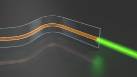
To remain competitive, companies will embrace heterogeneous integration – the integration on a single device substrate of different component technologies – and take advantage of the speed and performance of photonic chips. Transfer printed photonic chips have less packaging, are more efficient – with a high throughput rate per print cycle. They come at a much lower cost than a collection of separate optical and electronic components.

In an optical transceivers project, one of our European partners writes:
“CALADAN will develop integration technology based on Micro-Transfer Printing (mTP) of high-speed SiGe BiCMOS electronics and GaAs quantum laser x-chips onto Silicon Photonics wafers. The technology can integrate optics and electronics in massively parallel steps fully at the wafer level, thus significantly increasing the fabrication throughput and reducing manufacturing cost.”
MedTech Solutions
In-vivo data is collected directly from living tissue using an implanted device or a device worn on the skin. The miniaturization of the chips, plus the heterogeneous integration of sensors, power, and RFID chips, has expanded the possibilities for healthcare applications.
In-vivo biosensors are designed to enable continuous and real-time monitoring of target metabolites in biological systems, which provide communications into and out of the cell.

As more and more patients rely on data transmission from wearables and cellphones to monitor their health, our technology delivers biomedical x-chips to capture and transmit that data.
We partner with MedTech companies thru X-Celeprint’s new Design for MedTech Manufacture X-DMM™ Process. It’s a collaboration between life sciences and technology that clearly articulates the efficacy of the device and the manufacturing process for innovative, Class 3 devices. Learn more here.
More information

![]()
X-Celeprint is an international leader in micro-transfer printing. Our headquarters are at the Tyndall National Institute in Cork, Ireland. We also have a Development Center in Research Triangle Park, NC. We serve customers in North America, Europe, and the Asia Pacific. We provide our clients with design support, prototyping, printing, licensing, and tech transfer for commercialization.