Enabling Complex Integration Solutions

The integration of separately manufactured components to provide enhanced functionality. It’s what we do.

Heterogeneous Integration is the New “Tiny”

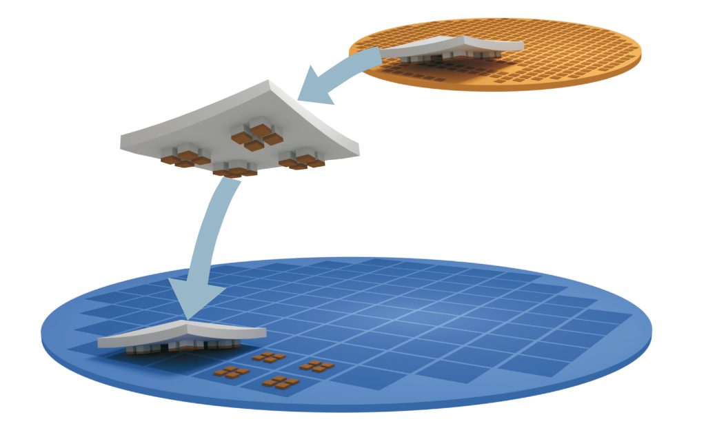
Heterogeneous integration is the process of combining separately manufactured components into a high-level assembly that provides enhanced functionality and improved operating characteristics.  Micro-transfer printing is a proven methodology for achieving it.

Target Applications For Micro-Transfer Printing

Pie Chart of Market
The semiconductor market is expected to reach $601 Billion in 2022
(Source:  WSTS Semiconductor Market Forecast Fall 2021)

Analog, optoelectronics, discretes & sensors

  • A $178 billion market in 2022
  • Not micro/logic /memory
    (The focus of heterogeneous integration to date)
  • Addresses megatrends driving semiconductor demand
    (5G, energy efficiency & artificial intelligence)

How do we help?

Every client has different technology requirements. Using micro-transfer printing, we can customize a design unique to each set of specifications.

The tight integration of large arrays of ultra-thin (<10mm) diverse components, SOI, SiGe, GaN, GaAs, InP, and passives enables:

  • RF communications
  • Power management
  • Photonics
  • Medical Applications

Depending on customer requirements, the final device can include high current density (RF and power transistors) or lower I/O density-  without ultra-fine interconnects – all in a very small form factor. The goal is to provide each client with the device they need for a successful product launch.

Photonics Light the Way

The demand for data is never-ending and instantaneous access is the goal to meet. With the coming of Artificial Intelligence (AI), Machine Learning (ML), Quantum computing, and data centers there is a challenge to meet the connectivity demands of billions of devices. Photons move at the speed of light without the interference that comes from electronic transmission.

With photons, data is transmitted faster and more efficiently, with lower latency and using less power.

Smartphones, tablets, wearables, automotive sensors, IoT devices and computers all rely on photonic chips.  Components are combined to expand the functionality of the chip without increasing the size, using minimal packaging and producing less waste.

Photonics Light

Heterogeneous Integration & Photonics

Using heterogeneous integration multiple tiny components – laser diodes, modulators, photo detectors, optical amplifiers, and optics – are precisely aligned on a single substrate, with wave guides on a wafer.

  • Efficient assembly of multiple heterogeneous materials
    Lasers, Modulators, Detectors, Driver ICs: analog and digital.
  • Precision alignment at each step
    Efficient coupling of devices to waveguide wafers
  • Mass Transfer
    Scales to high device count as performance demands continue to rise
  • Minimized device sizes
    Significant savings of expensive III-V materials

Let’s Talk MedTech

Not only does Micro-Transfer Printing enable many MedTech applications but X-Celeprint helps to speed the regulatory-approval process. The FDA’s average response time for an application related to a Class 3 medical device is 243 days. Class 3 represents the newest and most innovative devices coming to market.  A Premarket Approval (PMA) application requires presentation of scientific evidence that demonstrates the safety and efficacy of the device.

Any element in the process can be challenged, restarting the approval process all over again. Until the approval is granted, revenue generation is off the table: no label, no launch. 

Class 3 devices include MedTech wearables, lab-on-a-chip development programs, in vivo implants and any device that requires a photonic integrated circuit upgrade in the next 5 years. Anything that slows down the approval process slows down the launch of medical advancements.

MedTech Chip

Obstacles & Risks

Design verification is critical in getting an approval on the first attempt. The risk increases exponentially with implanted or diagnostic devices. So does the regulatory scrutiny of the FDA and EMA.

The length of time to market and immense cost involved in a Medical Device certification means companies can’t afford any mistakes.

X-Celeprint at Upcoming Conferences

ECOC Logo

European Conference on Optical Communication

Date:  September 22-26, 2024

Location: Congress Center Messe Frankfurt, Germany

Register here

iMap logo

Photonics West 2025

Date: January 25-30, 2025

Location: Moscone Center, San Francisco, CA

Register here

IPC Logo

Optical Fibers Conference 2025

Date: March 30 – April 3, 2025

Location: Moscone Center, San Francisco, CA

Register here

What X-Celeprint Offers

Our scientists and engineers are experts in the field of micro-transfer printing. Our goal is to empower chip designers and manufacturers through heterogeneous integration.

We specialize in the heterogeneous integration of silicon and compound semiconductors, including photonics, sensors, RF and power devices.

Our clients receive ongoing support as they move through the digital ecosystem. It’s our job to provide the expertise that our clients need to produce a high-quality chip that delivers for their customers and vendors.
SERVICES

  • Define Requirements: The first step is understanding the client’s requirements and objective for the device. NDAs protect confidentiality to protect intellectual property. 
  • Design support: We engage with clients to understand their end goals and provide guidance and recommendations on how best to achieve them.
  • Prototypes:  Clients need assistance developing prototypes. We help them through the process and assist in development of prototypes, particularly for our government clients.
  •  Printing and Production: Working in a cleanroom lab, the components are micro-assembled and printed in the chosen form factor. Precision alignment is key in heterogeneous integration.
  • Licensing: A license is required to implement and practice MTP. Our clients can secure a license to practice MTP at any time during the process although most wait until a prototype is developed and tested.
  • Tech Transfer for Commercialization: We have a large team of MTP experts and are ready to support you or a vendor under contract to scale up the technology to commercialization. We are also working with a number of potential vendors to supply print-ready components, print-ready targets, as well as provide MTP printing services.

X-Celeprint is an international leader in micro-transfer printing. Our headquarters are at the Tyndall National Institute in Cork, Ireland. We also have a Development Center in Research Triangle Park, NC. We serve customers in North America, Europe, and the Asia Pacific. We provide our clients with design support, prototyping, printing, licensing, and tech transfer for commercialization.

Let's Talk