
Micro-Transfer Printing Technology
What is Micro-Transfer Printing (MTP)?
MTP combines diverse, non-native components on a single substrate – silicon, paper, plastic, ceramic, or glass.
It has been proven to be one of the best method for achieving heterogeneous integration. Learn More.

Integration of compound semiconductors
Heterogeneous integration of compound semiconductors is a critical technology for advanced wireless communication, power management, optoelectronics and photonics, and sensor components. These have different requirements than logic and memory components.
Micro-Transfer Printing provides:
- Tight integration of large arrays of compound semiconductors (e.g., GaN, GaAs, SiC, SiGe, InP) with silicon (CMOS) semiconductors and passive components (inductors and capacitors) versus integration of chips having standard interfaces and made using different CMOS nodes.
- Lower I/O density and higher current density interconnects.
- Ultra-thin, small footprint three-dimensional integrated circuits (3D ICs) versus a large footprint system-in-package (SiP).
- Disruptive innovations that improve performance but don’t require scaling to advanced CMOS nodes or high I/O density silicon advanced packaging.


Inserting 3D IC compound semiconductor heterogeneous integration between wafer fabrication and packaging (Figure 1 ) enables many opportunities for disruptive innovation. 3D ICs improve the interconnects (reducing parasitics components, improving thermal management and power density) and bridge the dimensional gap between the wafer fabs’ ultra-fine (<1/1mm line/space) and packaging’s coarse (>10/10mm) interconnects.

Enabling Heterogeneous Integration
X-Celeprint delivers cost-effective production of 3D ICs that incorporate a wide range of passive and discrete components.
Thin (~10 microns) chips, dubbed x-chips, are lifted and transferred from donor wafers to CMOS or other target surfaces, providing wafer-level integration of:
- Discrete components: Analog/RF transistors, photonics, sensors, security
- Passive components: Capacitors, filters, antennas
- Different process technologies/nodes: SOI, GaAs, GaN, InP
Read our latest paper on 2022 08 Integrated Power Electronics Components for Integrated Voltage Regulators, published in the IEEE Electronics Packaging Society (EPS) e-newsletter

Less Waste, Minimal Packaging
MTP enables superior chip performance in the simple form factor of a monolithic IC wafer that is further processed
by a wide range of advanced packaging techniques for monolithic dies.
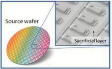
Step 1
Fabricate x-chip devices with a sacrificial
under-layer and tether system.
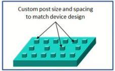
Step 2
Create custom tailored stamp to transfer devices
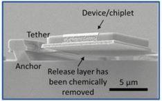
Step 3
Chemical etch of sacrificial layer on source wafer, creating suspended devices.
Step 4
Align stamp with devices to be transferred
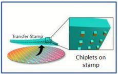
Step 5
Lift stamp and break tethers, removing devices.
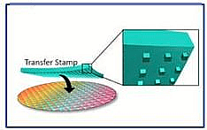
Step 6
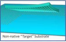
Stamp contacts target wafer and transfers the devices
Repeat the process for as many designs and devices as requested!
Devices can be moved from multiple wafers
Micro-Transfer Printing will transfer from more than one source wafer if desired, fanning out densely packed x-chips from the source wafer and interleaving them on the destination wafer.
Destination wafer layouts can be sparse or dense and still have very high utilization of source and destination materials.
Standard Interconnect and Packaging
After x-chips are transferred to the destination wafer using Micro Transfer Printing, standard BEOL thin-film metal can interconnect the thin x-chips on the destination wafer.
Thin x-chips and interconnects result in a thin near-monolithic die that is compatible with most advanced packaging techniques.


X-Celeprint is an international leader in micro-transfer printing. Our headquarters are at the Tyndall National Institute in Cork, Ireland. We also have a Development Center in Research Triangle Park, NC. We serve customers in North America, Europe, and the Asia Pacific. We provide our clients with design support, prototyping, printing, licensing, and tech transfer for commercialization.